Trying out the ice4pi from Lightside Instruments
As I mentioned in my Kilnettle Tape Dispenser post, some of my favourite things about in-person events are the wee conversations that happen in the corridors and hallways around the event itself. I was lucky enough, at the recent Open Hardware Summit, to run into Vladimir from Lightside Instruments and chat to him at their table, showing off some of their interesting Pi and FPGA-based circuits and projects.
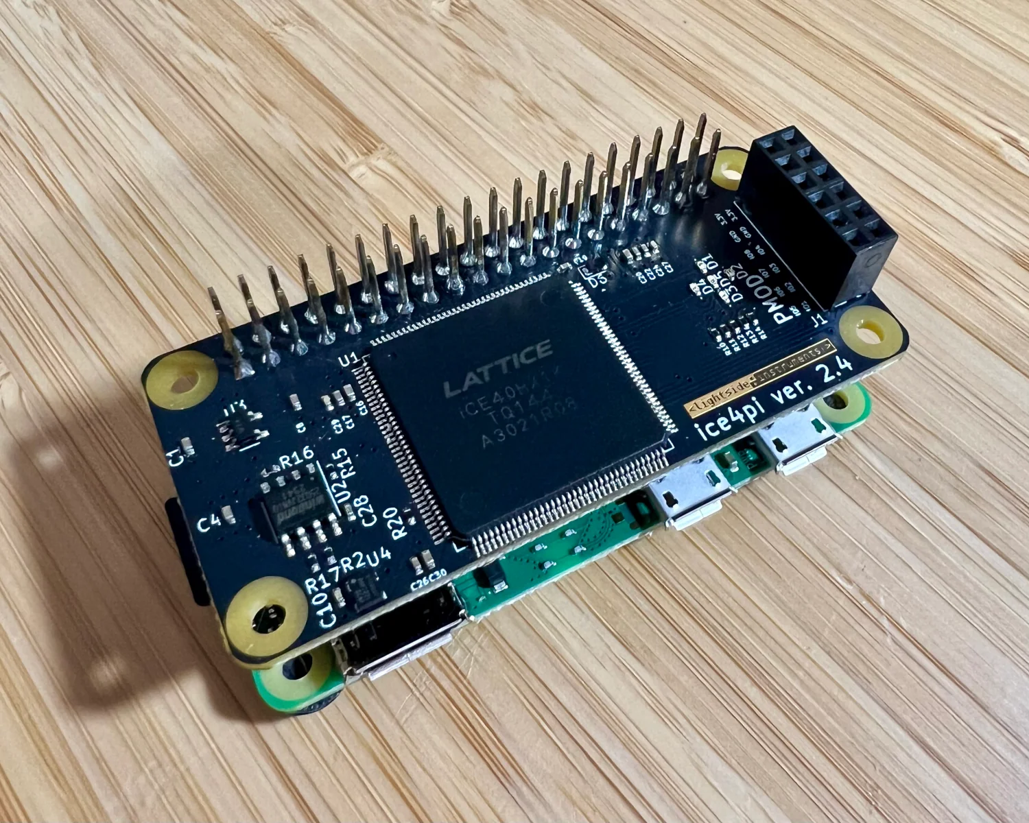
He was kind enough to gift me one of their ice4pi iCE40 shields for Raspberry Pi format single-board computers.
Out-of-Box Experience
Lightside Instruments have provided a pretty decent walkthrough on hackster.io to get you set up, and what follows here is basically just my re-telling of their story.
First things first, let's get an operating system flashed on to the Pi.
It's been years since I've set up a Pi, and the last time I did, it involved /boot partitions and wpa_supplicant files to get a headless Pi onto your Wi-Fi.
It turns out that the "2025" way to do this is with the official Raspberry Pi Imager tool.
Use the imager tool to burn Pi OS Lite (64-bit) to a MicroSD card with your settings, then boot and log in.
To get the ice4pi up and running, the first task is to enable SPI on the Pi, so we can talk to the FPGA for programming.
This can be done from within the raspi-config tool. Once enabled, shut the Pi down, so the ice4pi can be safely connected.
sudo raspi-config
# Enable SPI
sudo shutdown now
The ice4pi can now be safely connected, pushing it down firmly on to the 40-pin connector. Start the Pi back up, and the project's dependencies can be installed.
The example code files are downloaded with Git, and the other packages are the FPGA tool-chain.
sudo apt install git yosys fpga-icestorm arachne-pnr flashrom
Clone the project, enter the example directory and build it to turn the verilog code in to a flashable image.
git clone https://github.com/lightside-instruments/ice4pi.git
cd ice4pi/example
make
Load it on to the ice4pi using sudo permissions, and it should be good to go!
sudo make load
Custom Code
To prove we didn't just get lucky with the out-of-box example, and to further to ensure our environment's set up right, we can build the simplest project ever; a single jumper. From python on the Pi, we can blink one of its GPIO pins on and off. We can then write a small verilog program to connect that GPIO pin to one of the LEDs on the ice4pi through the FPGA.
GPIO 17 can be toggled on and off every two seconds with the following Python snippet, using the GPIO Zero library.
from gpiozero import DigitalOutputDevice
from time import sleep

out = DigitalOutputDevice(17)

while True:
    out.toggle()
    sleep(1)
GPIO 17 is pin 11 on the 40-pin connector, and according to the ice4pi's schematic, GPIO 17 (pin 11) is known by the net name PIO0_18.
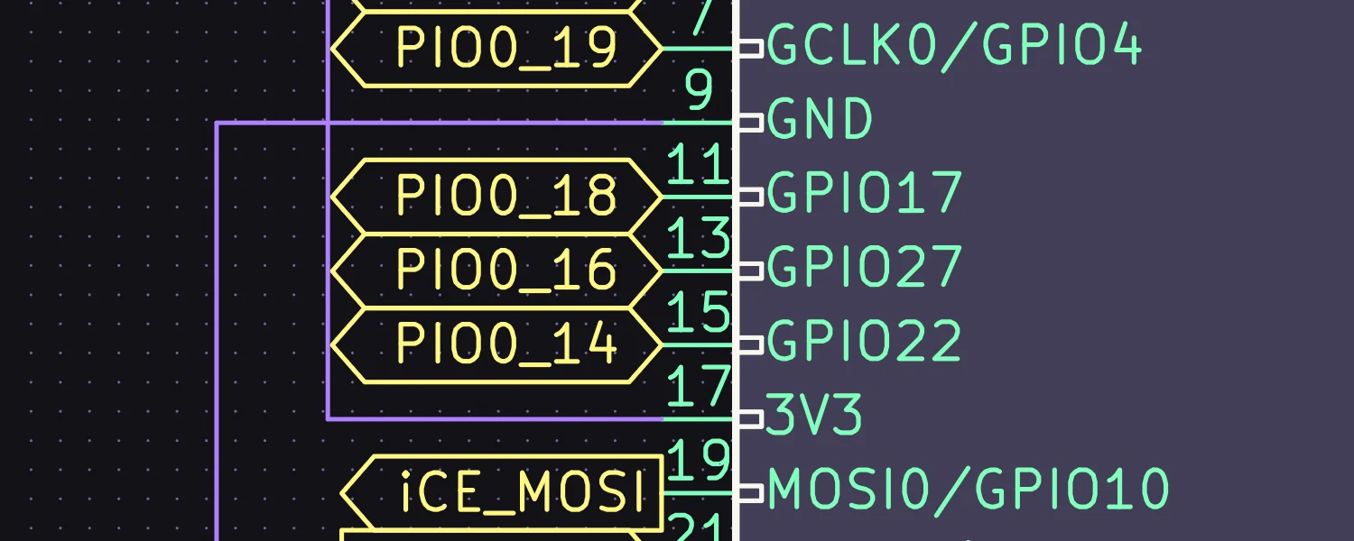
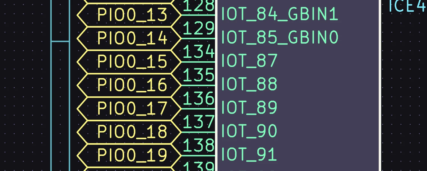
Following the net PIO0_18 on the schematic, we can find it connected to pin 137 on the FPGA.
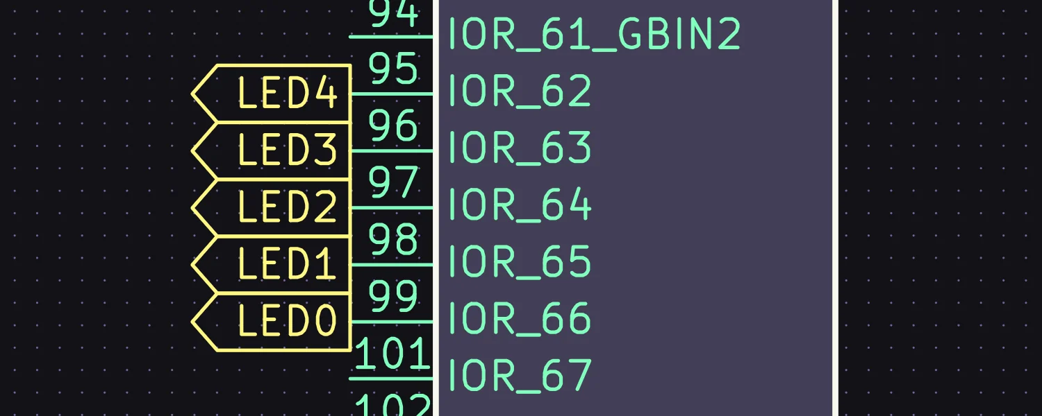
We can also find LED 0–5 on pins 99–95 on the iCE40 chip.
A pcf file that will make the GPIO and LED pins available to the verilog code as sensible variable names is just two lines long.
set_io PI_IN 135
set_io LED_OUT 97
With those definitions we can then write a very simple "one-liner" in Verilog to connect the Pi's GPIO to the LED.
module top(input PI_IN, output LED_OUT);

   assign LED_OUT = PI_IN;

endmodule
Running sudo make load again, will build our new, minimal, code file and load it on to the iCE40. If we then launch the earlier example Python script, the LED on the ice4pi blinks.
R-2R Ladder DAC Driver
I've been playing with R-2R Ladder DACs in recent posts, so I thought I'd bring one out again and see how well I could drive it from an FPGA. Referring back to the ice4pi schematics, there are 3 adjacent GPIO pins on the 40-pin connector which would be perfect for running our little 3-bit DAC.
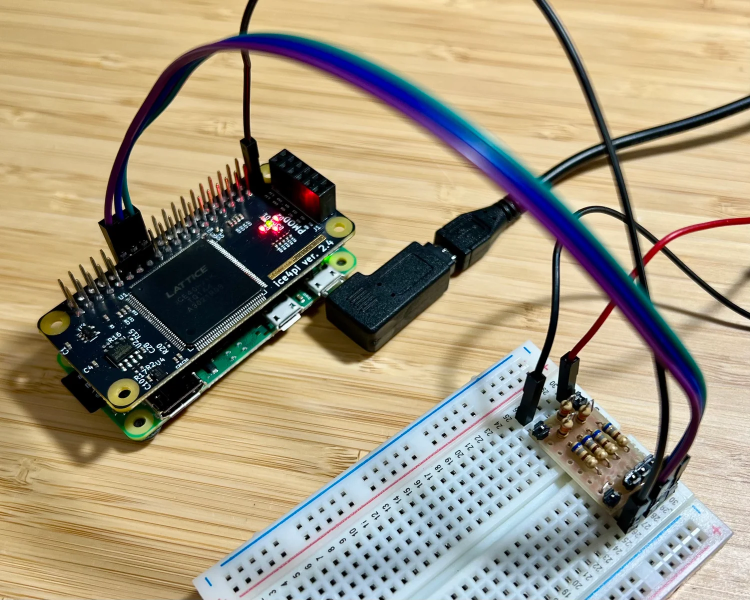
Following the net-names PIO0_14, PIO0_16 & PIO0_18 from the 40-pin connector brings us to pins 129, 135 & 137 on the FPGA. Pin 21 is connected to the 12 MHz clock crystal, which we'll need if we're to pass time accurately.
set_io clk 21

set_io DAC1 137
set_io DAC2 135
set_io DAC3 129
We can increment a 3-bit register, discarding overflows, to recreate our ramp wave from previous blog posts. Incrementing this register 300 times a second (once every 40,000 clock ticks) will result in a wave with a frequency of approximately 38 Hz. The three output bits can be connected to each of the three bits in our counter register.
module top(input clk, output DAC1, output DAC2, output DAC3);

   reg ready = 0;
   reg [23:0]     divider;
   reg [2:0]      counter;

   always @(posedge clk) begin
      if (ready)
        begin
           if (divider == 40000)
             begin
                divider <= 0;
                counter <= counter + 1;
             end
           else
             divider <= divider + 1;
        end
      else
        begin
           ready <= 1;
           counter <= 0;
           divider <= 0;
        end
   end

   assign DAC1 = counter[0];
   assign DAC2 = counter[1];
   assign DAC3 = counter[2];

endmodule
Hooking up an oscilloscope to the output of our 3-bit, R-2R Ladder DAC, confirms we've generated our ramp waveform.

Interestingly, we see no evidence of the glitches previously observed during bit transitions. I wonder if this means all three bits are being updated in parallel on the FPGA, where as there were clock ticks between each bit on the previous microcontroller versions.
2025-06-28