Back 2 Basics - Op-Amp Buffer
In my last Back 2 Basics post we built a DAC from an R-2R ladder. We managed to toggle its pins with an ESP32 and show that it could produce an acceptable analogue signal from just three bits of input.
This circuit works under test, but it would fail in real life, like when connecting it directly to a loudspeaker. Oscilloscope probes have a typical impedance in the megaohm range and have minimal impact on the measured signal. Loading the DAC's output with something in the 10s-100s of ohms pulls the voltage down dramatically.
We can see the difference here. The circuit connected to the high-impedance probe remains unchanged. The circuit loaded with a small resistor has dropped its output to below 10mV, or about 1/500th of its unloaded value.
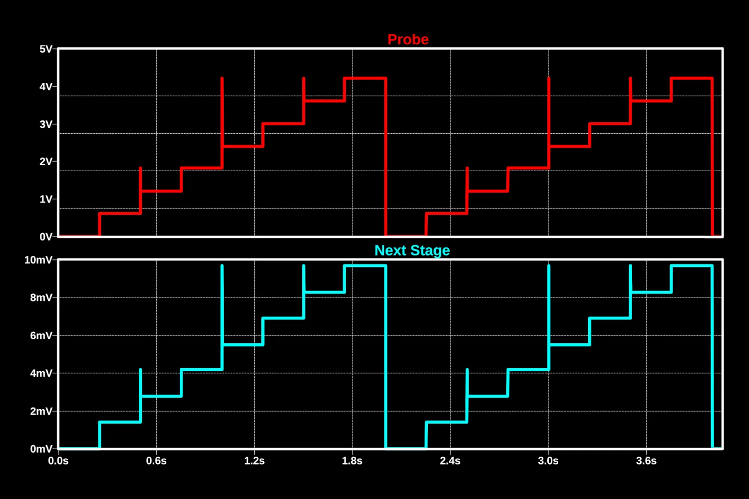
If we connected a loudspeaker, with an impedance of typically around 4 or 8 ohms, the signal would be inaudible.
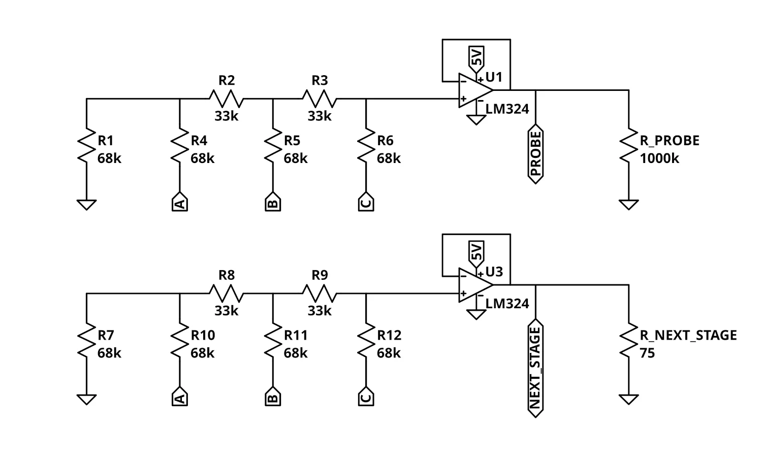
To reduce the impact of loading down the DAC, we can make use of a circuit called an Op-Amp Buffer, also known as a Voltage Follower. The buffer doesn't amplify or attenuate the signal, it just increases the range of impedances that can be connected between stages in a signal path.
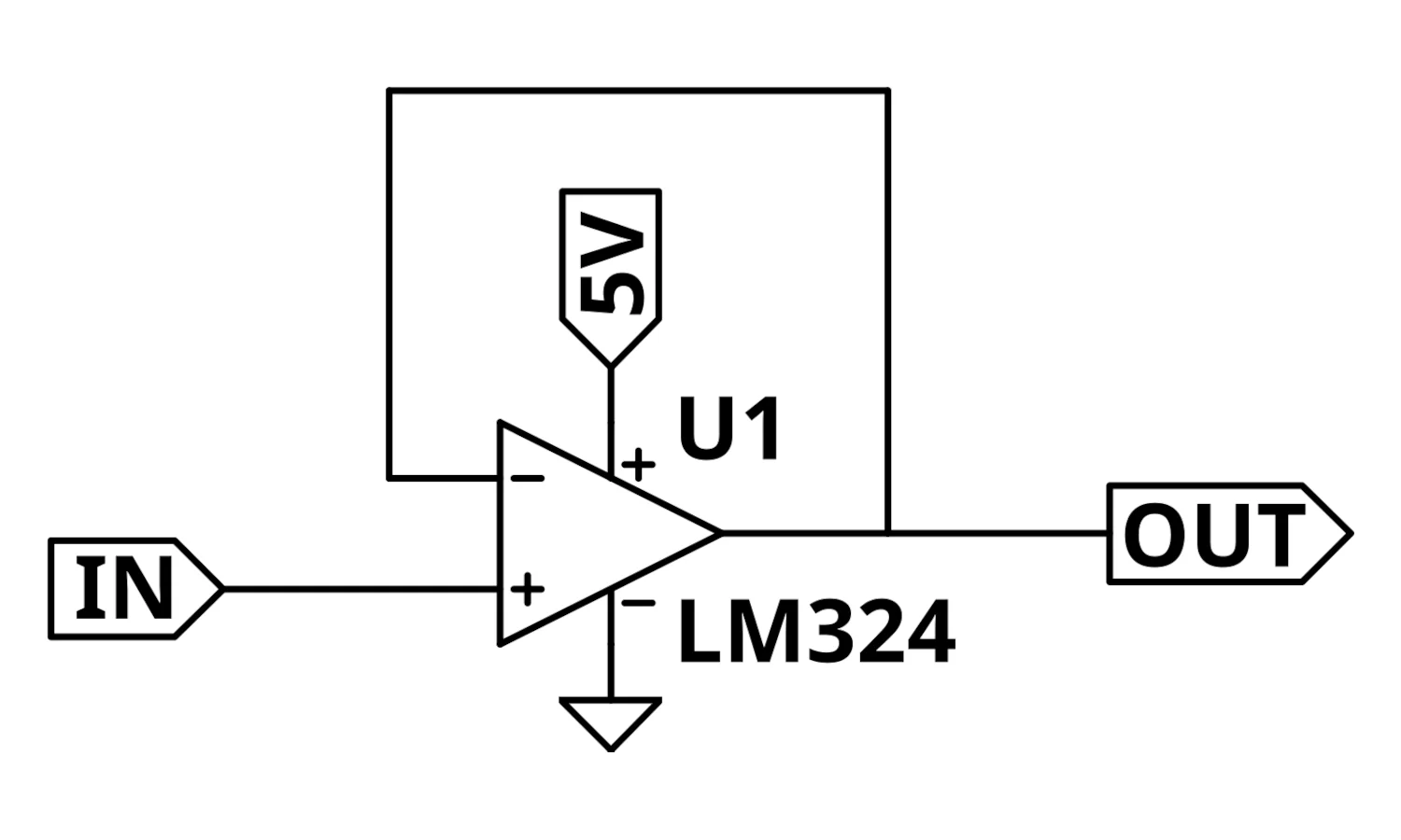
One model of Op-Amp that's commonly available to the maker or hobbyist community is the LM324. It's unlikely to see much commercial use these days as it's got fairly mediocre performance, but it's cheap, well-known, and available in easy-to-breadboard DIP formats. It won't operate rail-to-rail, but it has enough overhead to buffer 3.3v signals without distortion if it's powered from 5v.
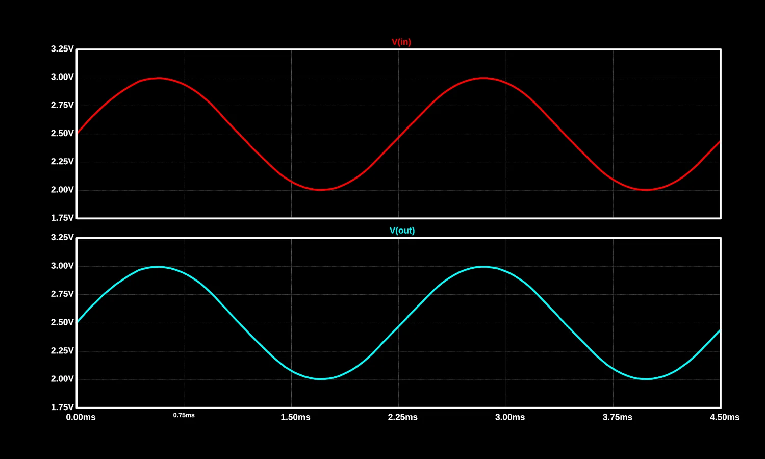
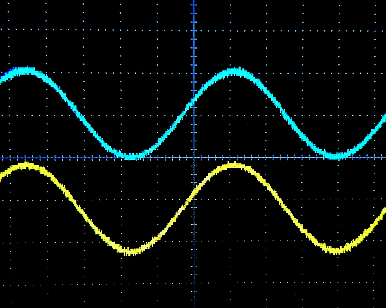
We can see the voltage-following nature of the buffer by sending a 1v peak-to-peak signal through the op-amp. Identical 1v peak-to-peak signals can be measured at the op-amp's input and output.
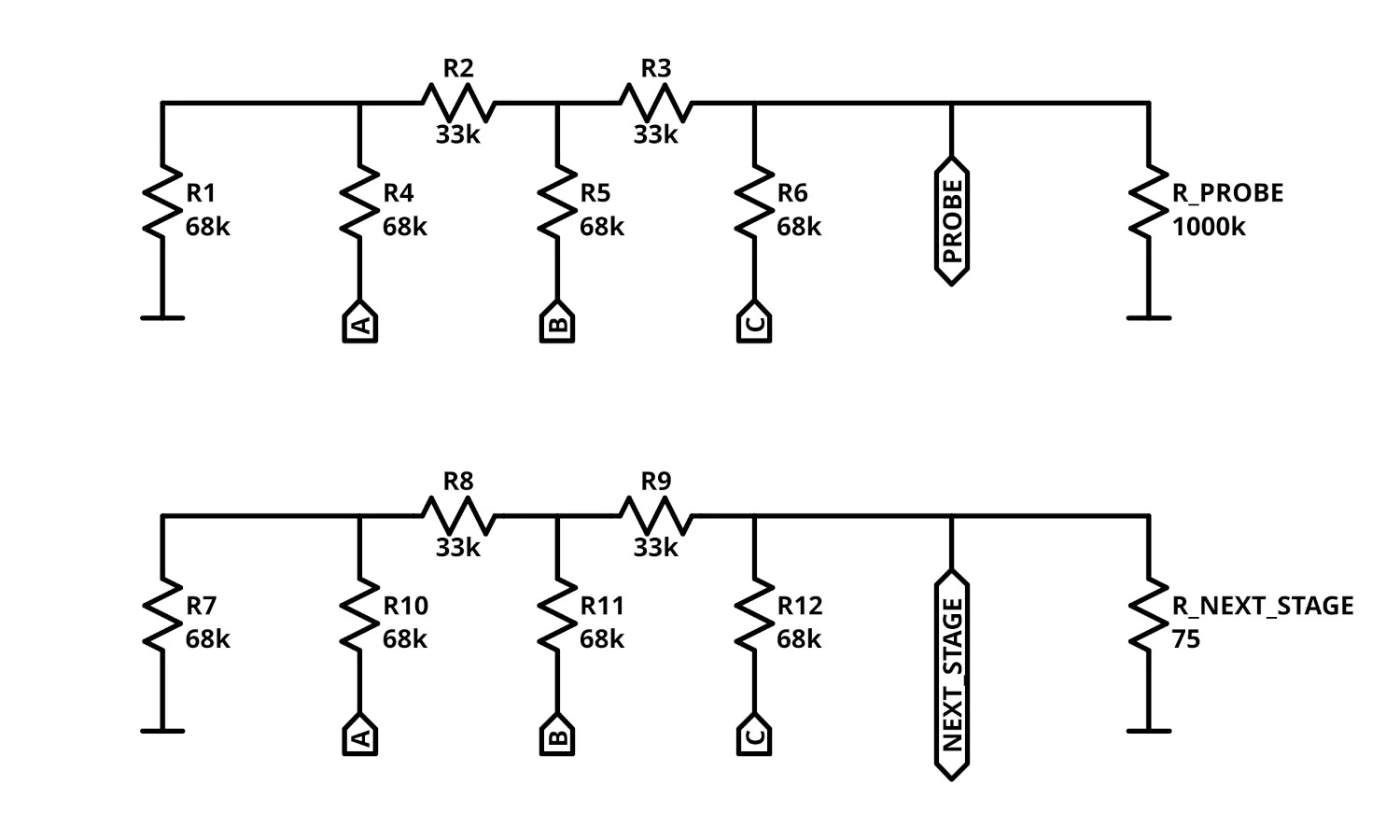
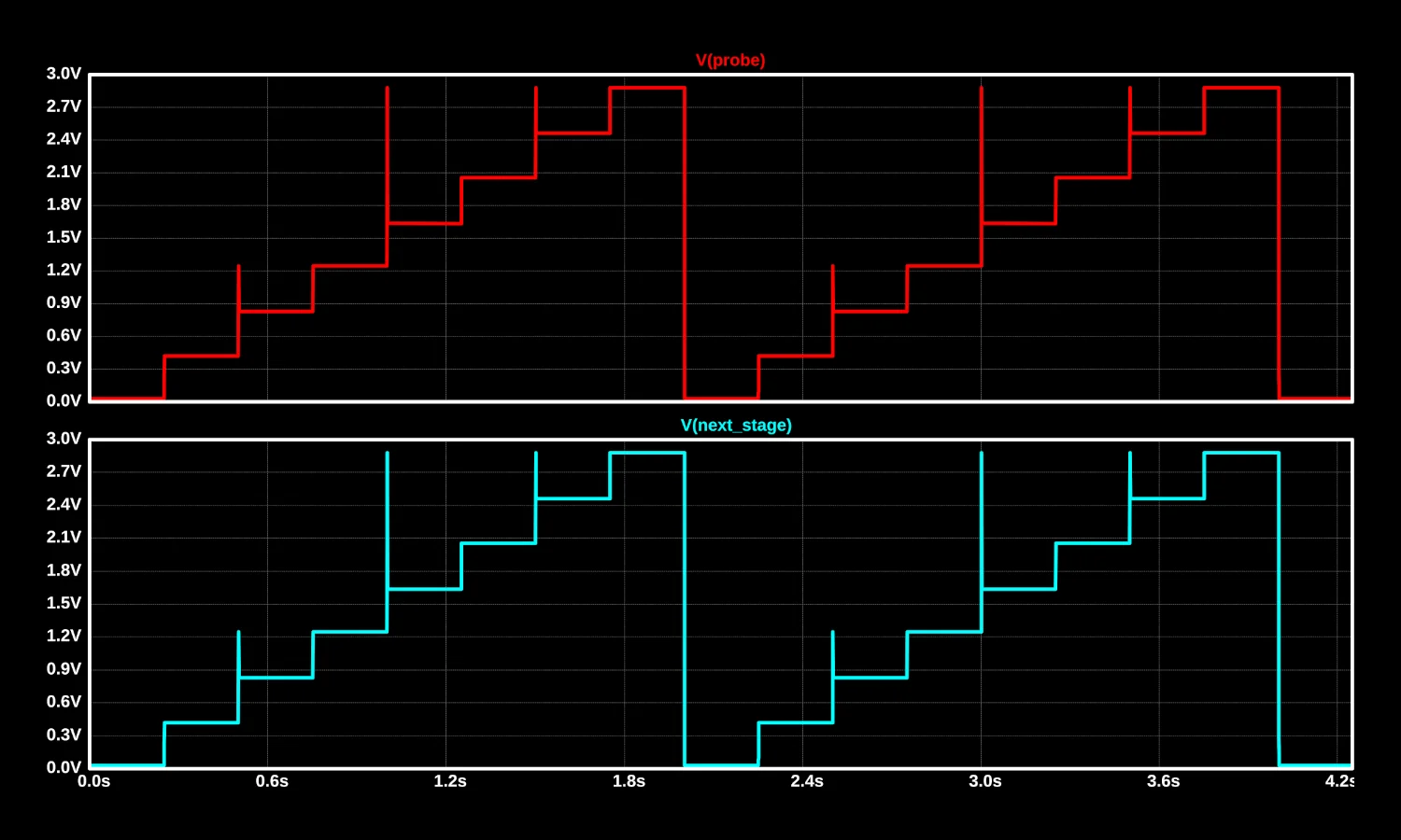
The example DACs from earlier can be rebuilt with buffers between their R-2R ladders and loads.
Measuring the output of both buffered DACs shows identical voltage levels despite the difference in loading.
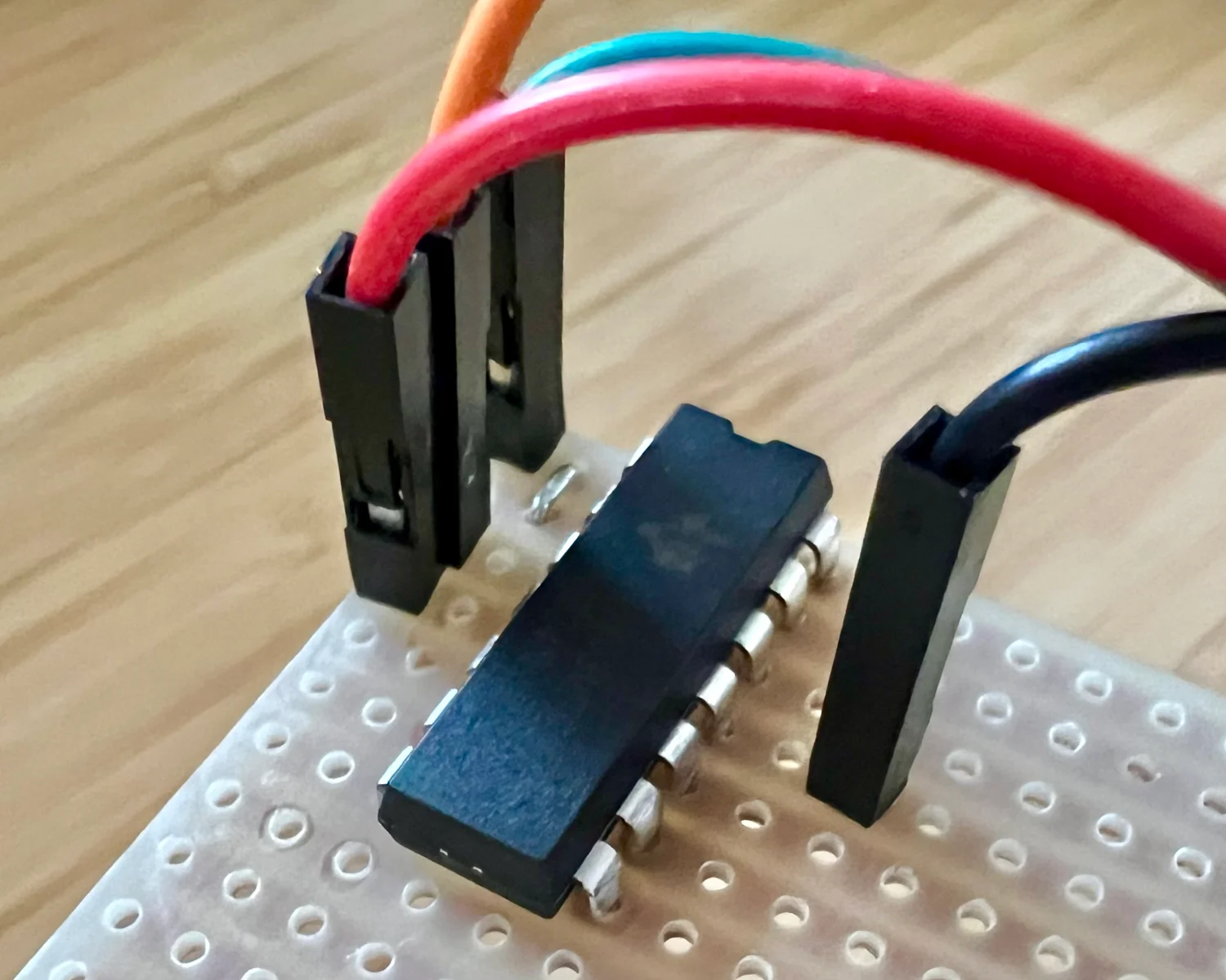
Building the real version of the buffer circuit is as simple as following the design in the simulation. Connect a jumper between the output and inverting input of a single op-amp in the quad package, then wire up the positive and ground supply and the input and output wires.
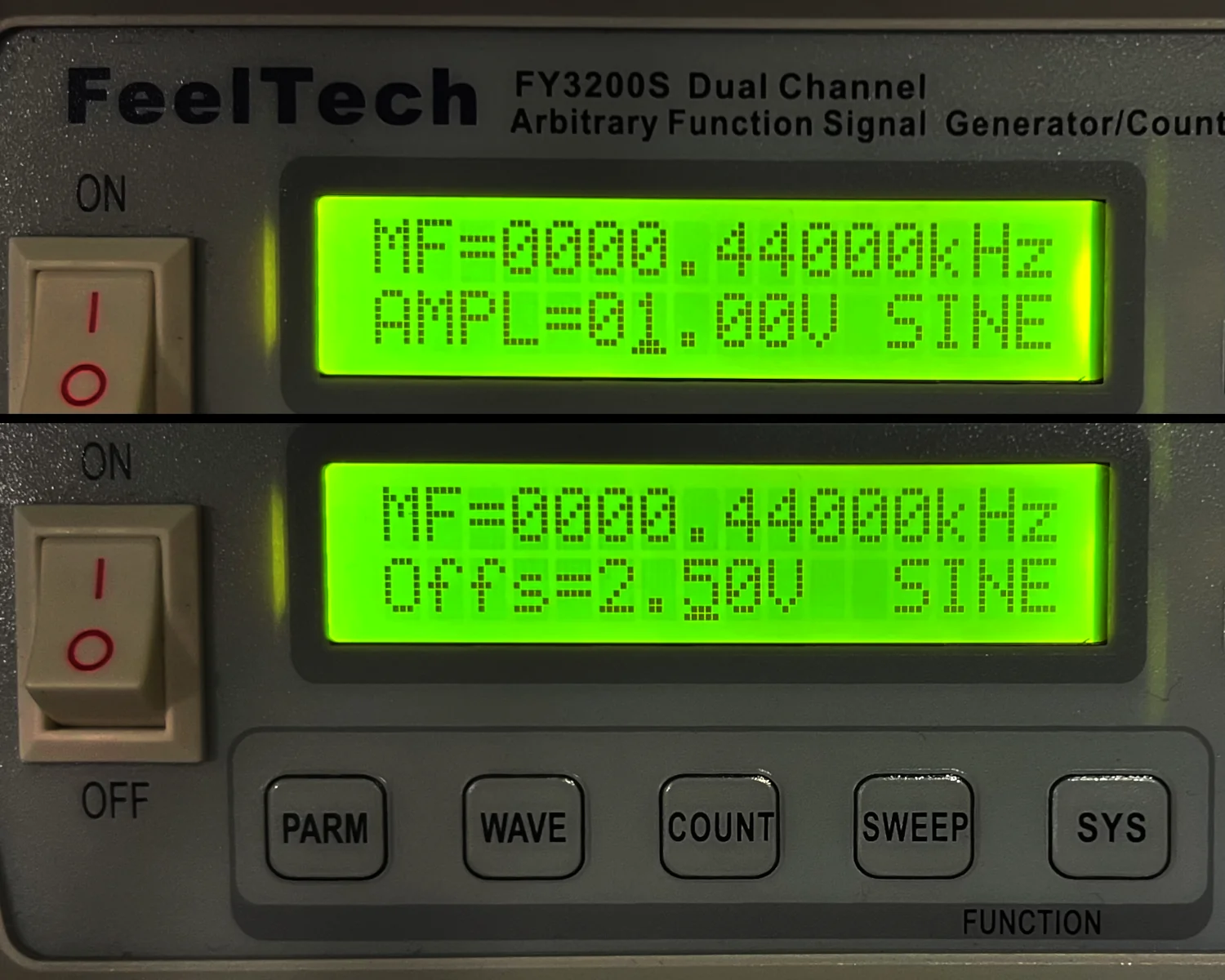
To test out the op-amp buffer, connect a signal generator to the input, then measure both the input and output using two channels on an oscilloscope.
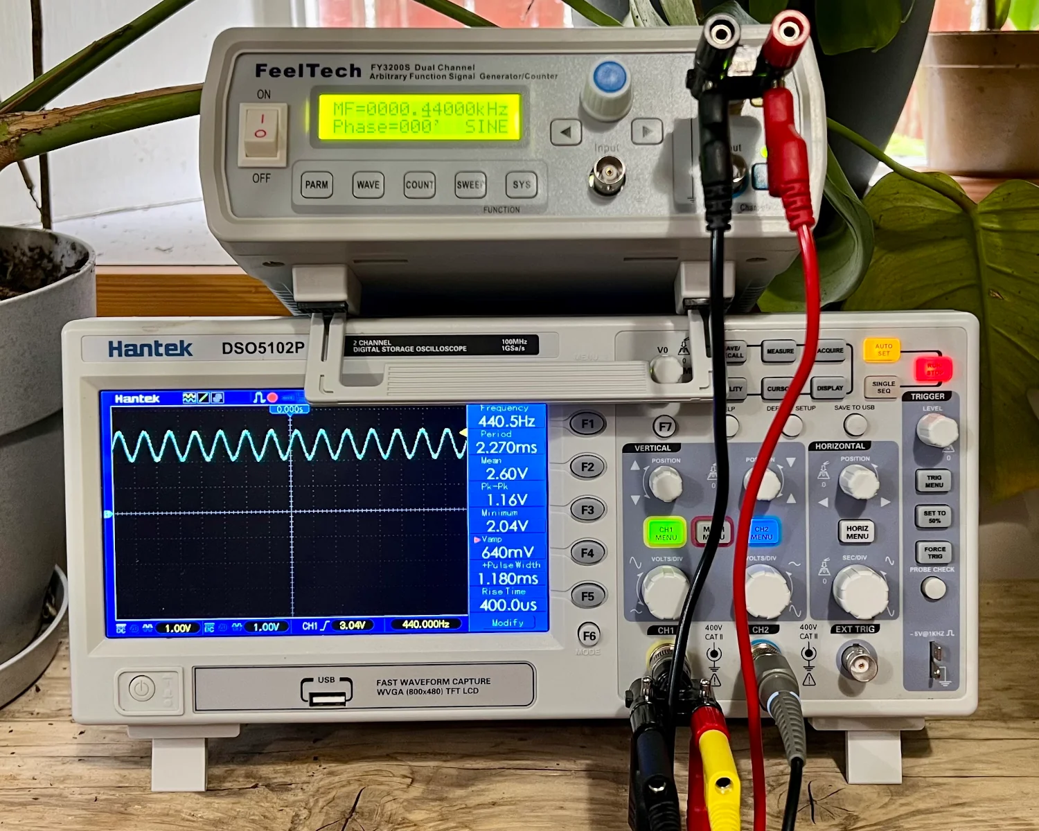
Running from a 5v power supply, the LM324 will operate between 0v and approximately 3.5v. The signal generator can be configured to produce a signal with 1v peak-to-peak, centred about 2.5v. This will generate a signal between 2.0v and 3.0v, well within the op-amp's range.
On the oscilloscope, we can see the input and output signals are identical, just like in the simulation earlier.
We can likewise improve the R-2R Ladder DAC from the last post by including this buffer, following the schematics from these simulations. To give a more practical example, I updated my ESP32's firmware to produce an "A" power chord.
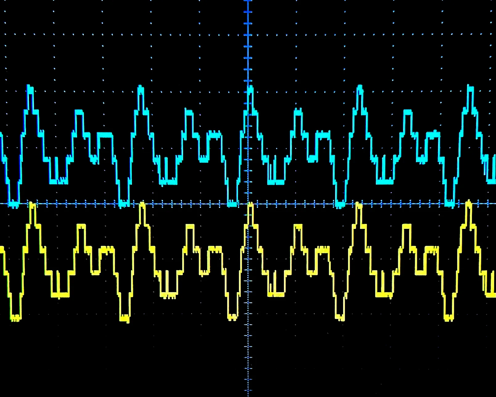
Identical signals can be seen at the buffer's input and output pins with the oscilloscope.
2025-06-23