Back 2 Basics - NMOS Switch
The last two Back 2 Basics posts were very much grounded in the analogue domain. This time we're going fully digital and looking at NMOS Switches.
If you've got a microcontroller with 3.3 or 5 volt GPIO pins and need to switch much higher voltage loads, or loads with high current drain, there are a number of components you could draw on. There are BJTs and JFETs, but one of the simplest to understand and easiest to implement is the NMOS, or N-channel enhancement mode Field-Effect Transistor.
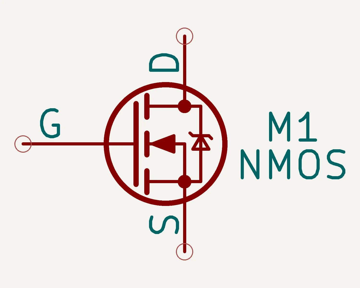
At its simplest, the NMOS switch can be considered as if it's just a voltage-controlled switch or resistor. Apply a small voltage to the Gate pin to turn the switch on, apply 0 v and it turns off again; swinging between being an almost 0-ohm short-circuit and a practically infinite-ohms wire-break. It is slightly more nuanced than that, but it doesn't take too much consideration to build it in to a working circuit.
Turning the NMOS on and off with a microcontroller lets us turn a large load placed between the supply rail and the NMOS' Drain pin on and off, as can be seen in this naive example.
The nuance comes from the practicalities of how MOSFETs are built. There are data sheets and formulas to work this out correctly, but if you want to "vibe" it out, here's the gist. There's capacitance between the pins which means we need to control our voltages and current flows a little.
When you turn the NMOS switch on, by applying a voltage between the Gate and the Source, you charge up that gate capacitance with current from your microcontroller's GPIO pins. Without a resistor in-line, you could pull much more current than your microcontroller will allow safely. In LTSpice simulations I've seen spikes as high as 150 mA. In the following circuit, Ru restricts the inrush current to less than 5 mA.
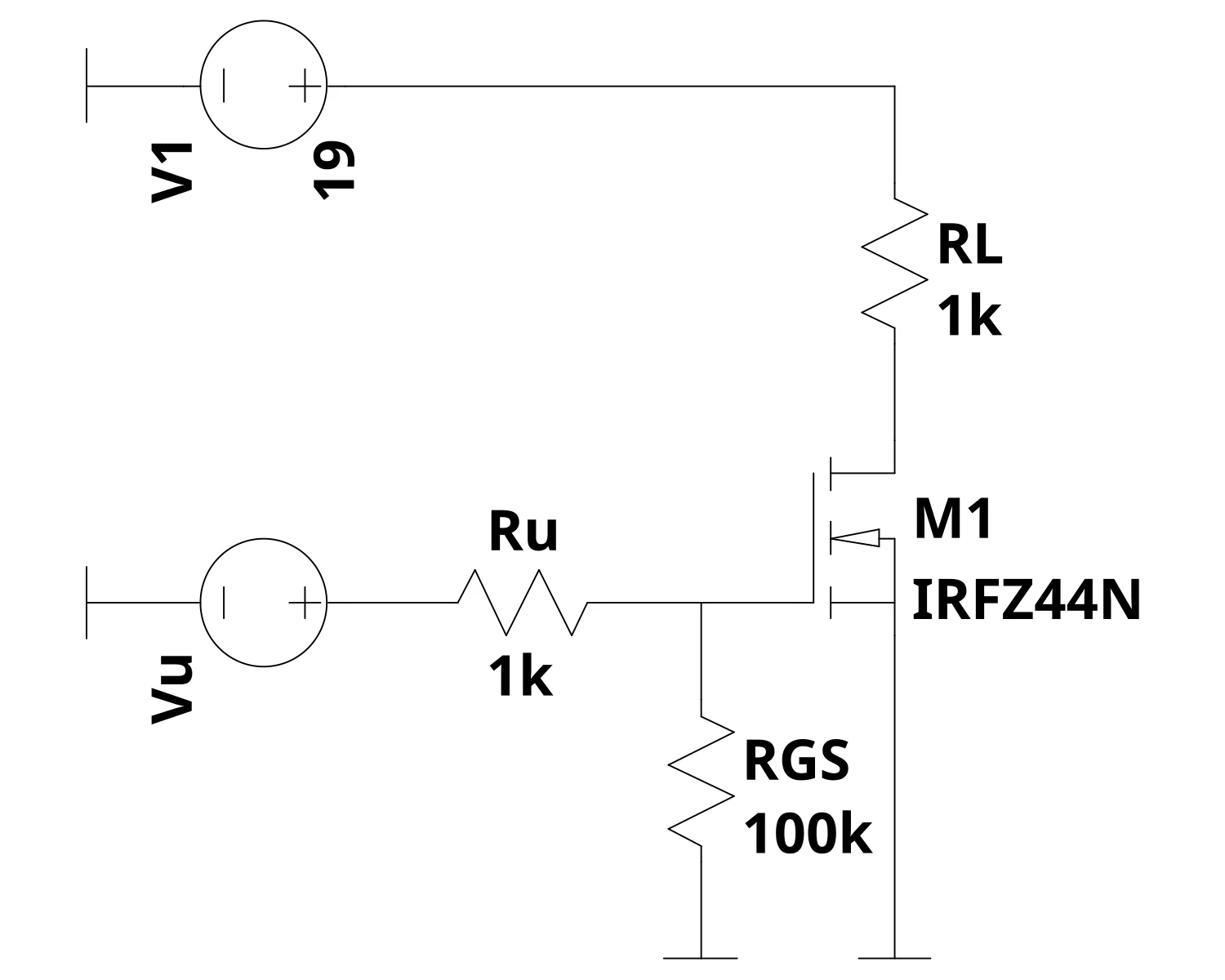
The capacitance between the pins also means that once you pull Vgs high, it could stay on until it naturally discharges below its threshold. If you use a solderless breadboard, there is extra capacitance found between the rows, so floating and latching false positives are even more likely. RGS in this circuit provides a path for this accumulated charge to dissipate. Tuning these resistors' values will control the switching speed of the circuit.
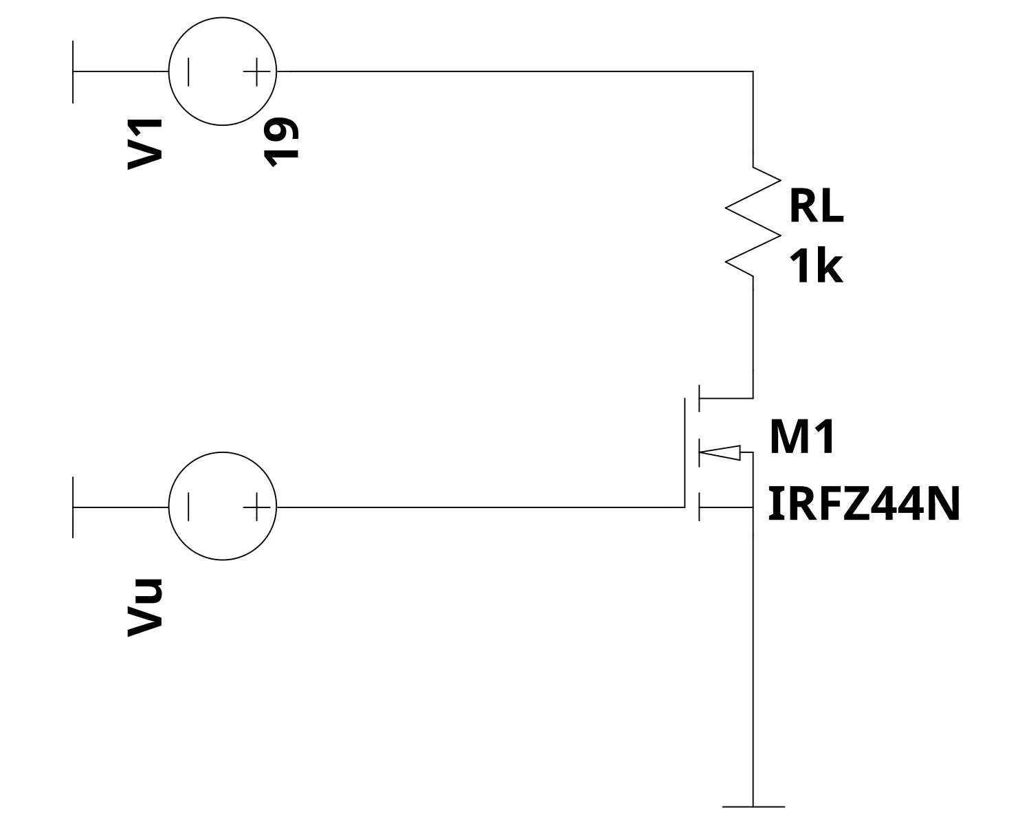
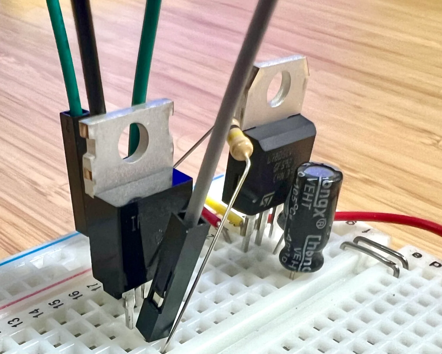
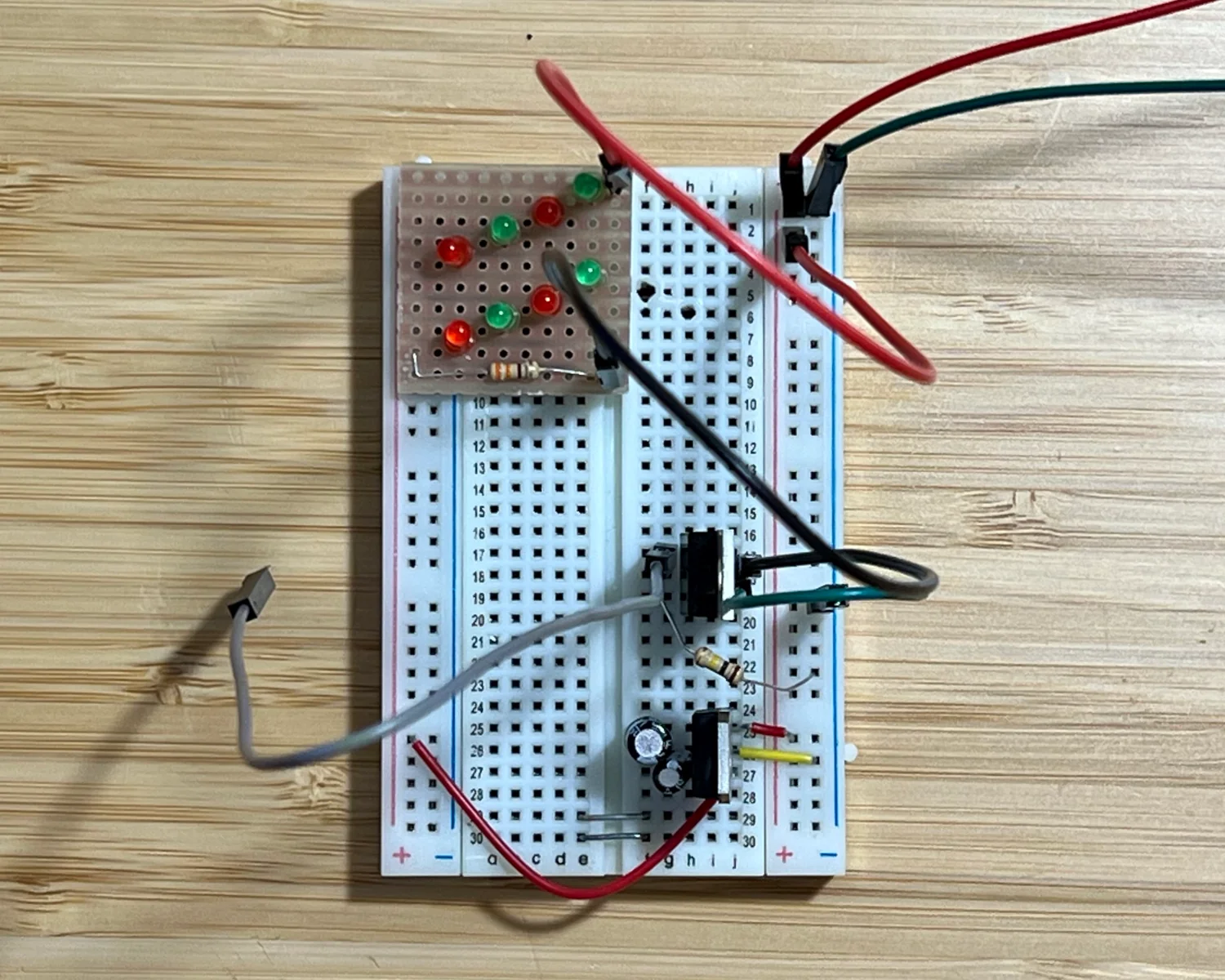
Now we've understood (or handwaved away) the theory of N-channel enhancement mode MOSFETs, we can build one in to a real circuit. The following circuit will allow us to switch a 19 v load from a signal voltage of just 5 v, or less. I've included a small LM7805 circuit to provide that 5 v switching signal from our 19 v supply.
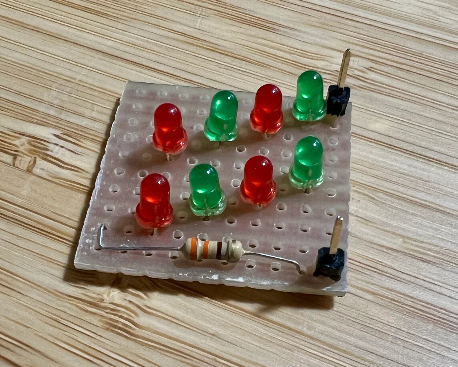
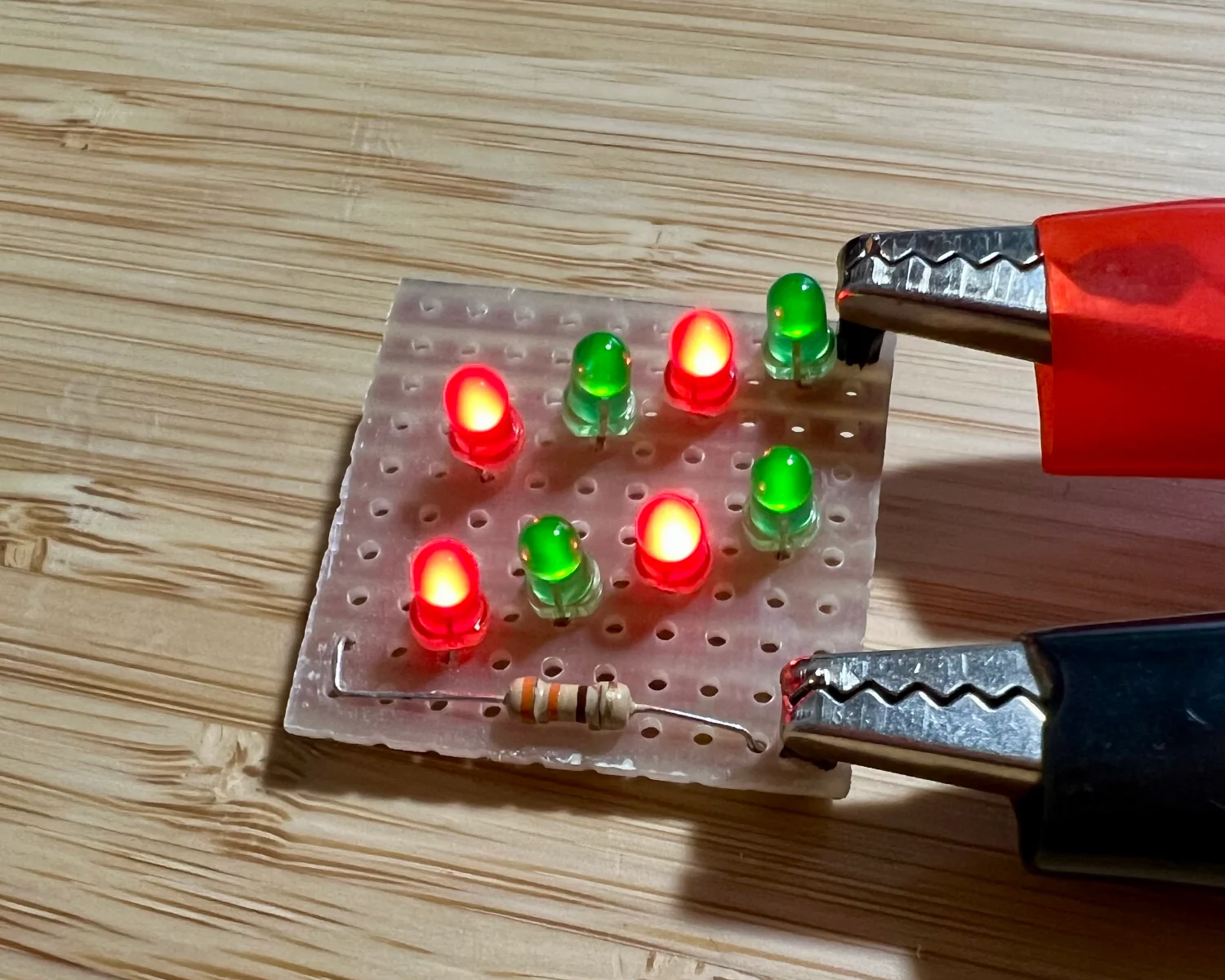
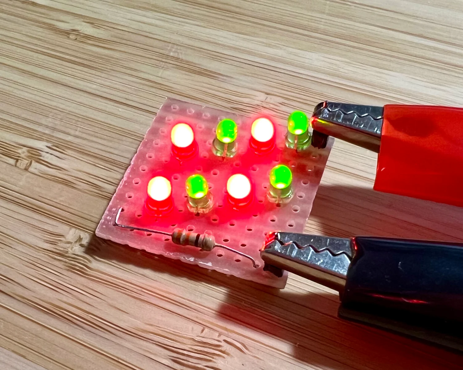
The 19 v load consists of 8 LEDs, all with forward voltages in the 1.8 to 2.1 volt range, and a small amount of resistance to restrict the current. It will begin to turn on at about 15 volts but really needs the full 19 v to fully shine.
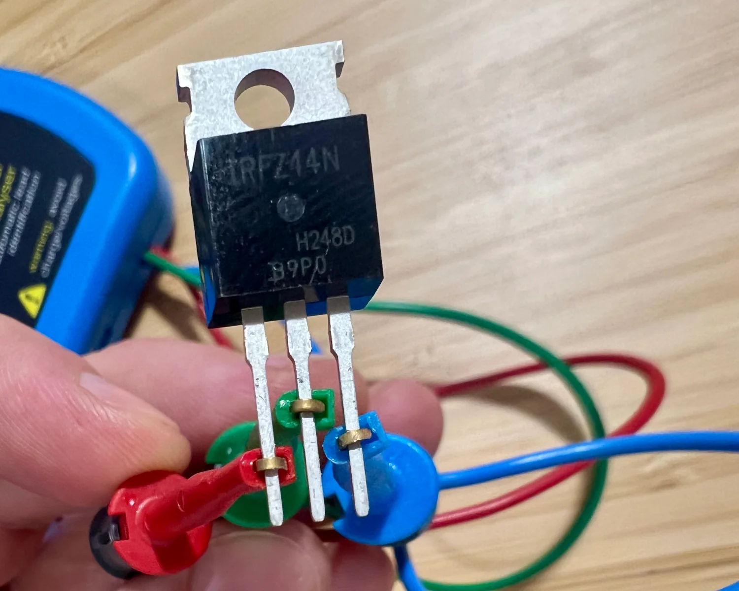
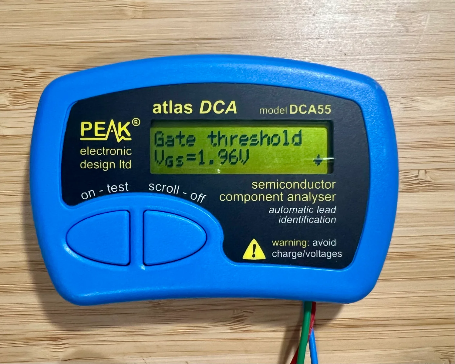
I've chosen the IRFZ44N here as it has a simulation model already defined in LTSpice and is commonly available for makers in hobbyist parts kits. A suitable alternative would be the 2N7000, which is also commonly available to hobbyists and has a SMD variant in the 2N7002 if you want to have it assembled on a PCB.
Building the IRFZ44N in to this roughly breadboarded circuit lets us test out toggling a 19-volt load with a 5 v signal.
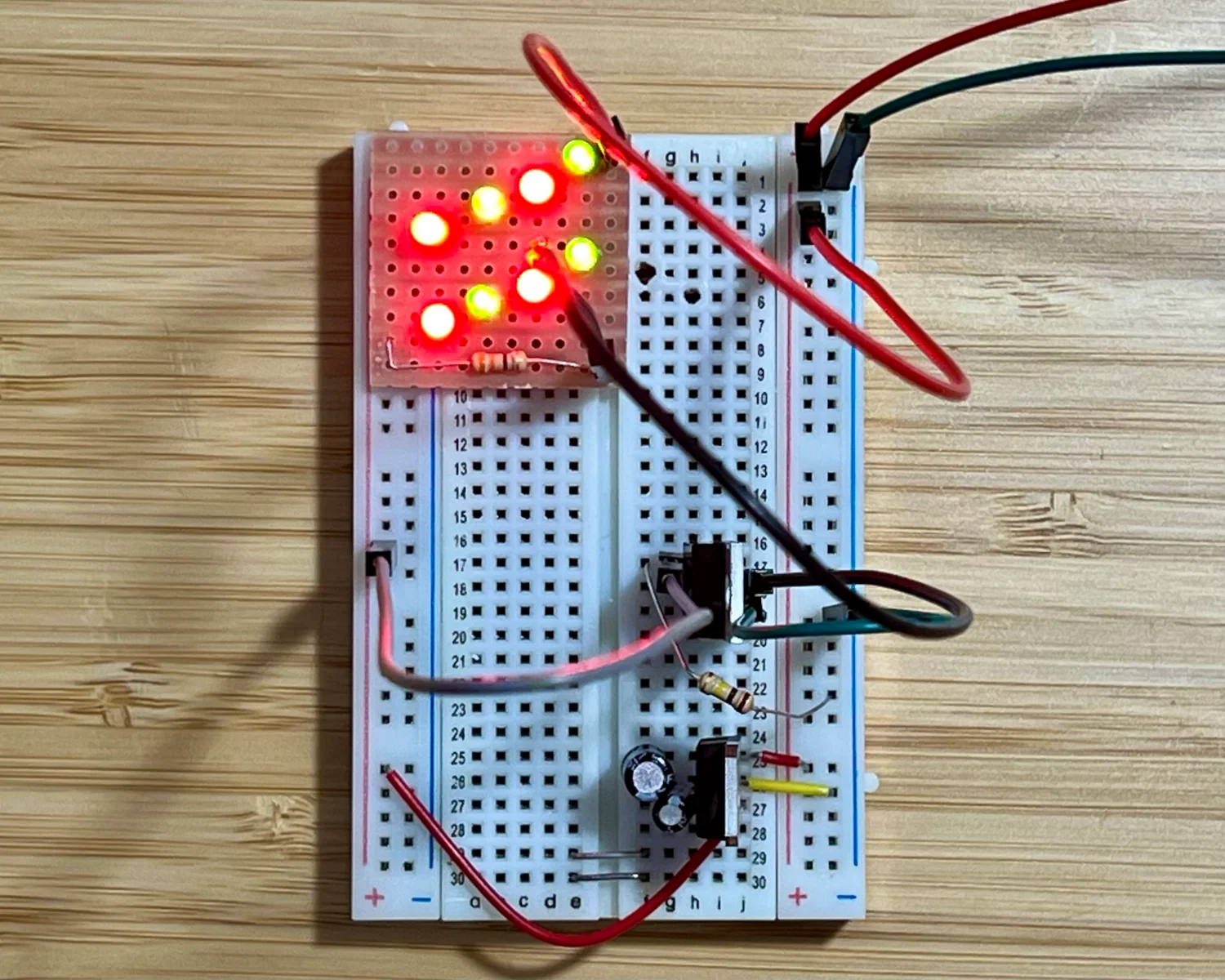
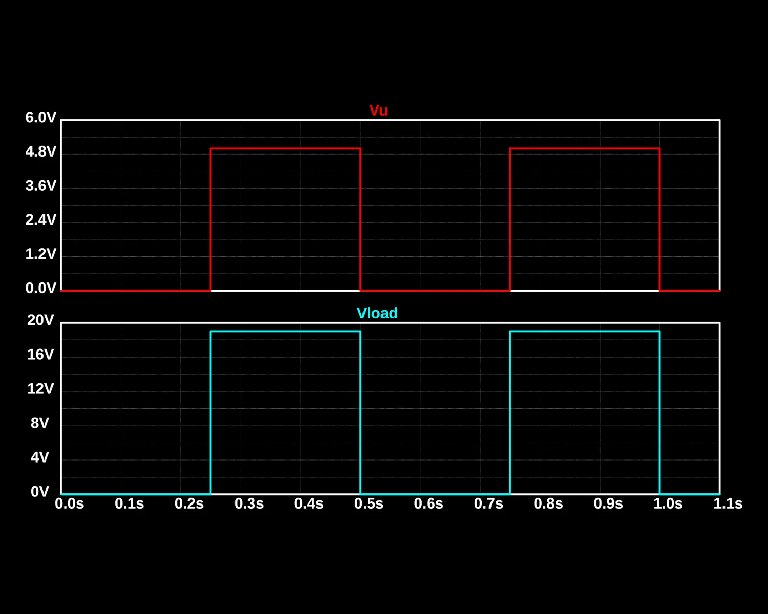
RGS pulls the gate to ground; holding the NMOS in the off position and keeping the load shut down. Connecting the gate to 5 volts brings Vgs above its threshold, turning on the NMOS and letting current flow through the load. We're now able to switch "higher" voltage loads from microcontroller GPIO pins.
All the supporting circuit simulations performed above can be found in my back-2-basics repository.
Now, with our newfound knowledge of NMOS switches, let's find a practical application...
2025-07-20